1. Same-Channel Full-Duplex Radios
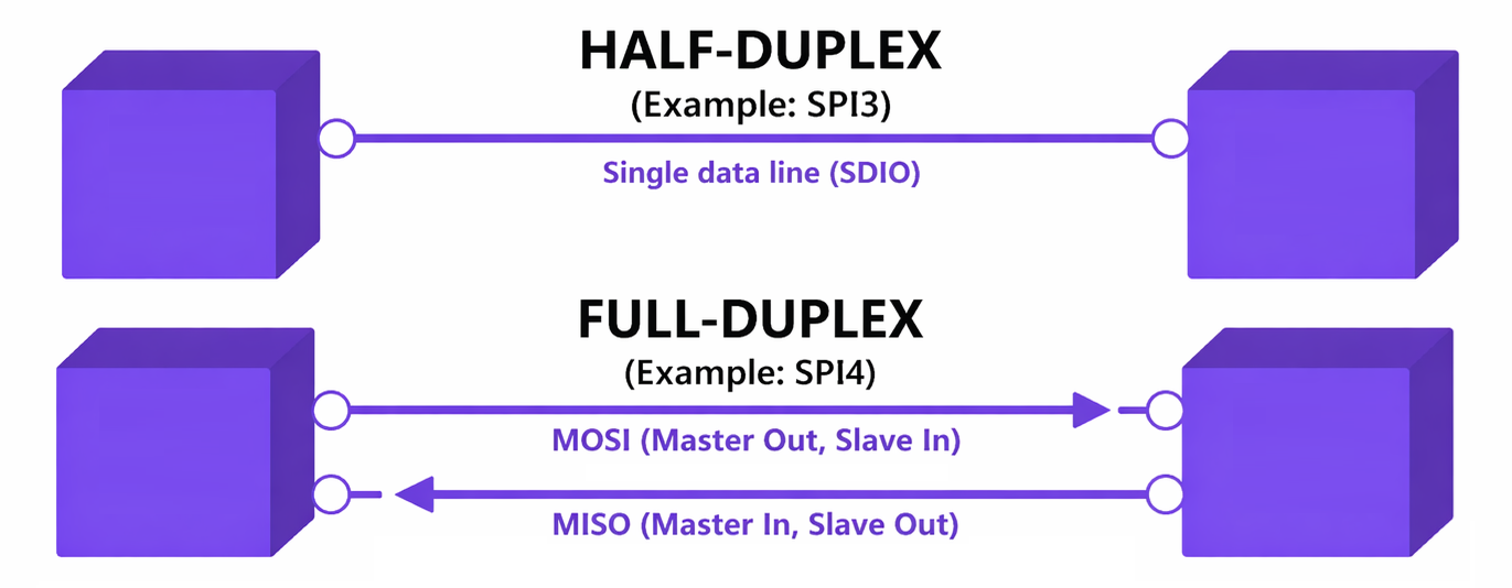
"Duplexing" refers to the establishment of a two-way communication between two nodes. Conventionally, digital copperline protocols were classified as "half-duplex" where the same wire is shared on the basis of taking turns, and "full-duplex" where two dedicated wires are used.
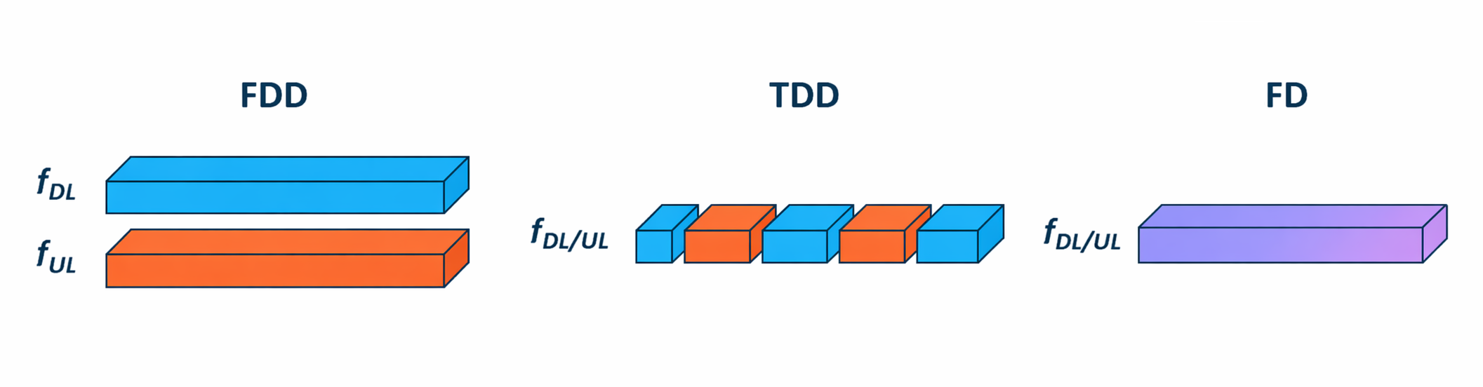
Radios in modern communication systems are classified into time-division duplex (TDD), frequency-division duplex (FDD) and full-duplex (FD). TDD uses the same frequency band but assigns different time-slots for sending and receiving. FDD uses two different bands for simultaneity. FD uses the same band to send and receive at the same time.
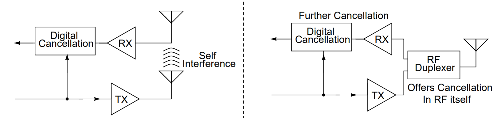
When we have two antennas, the self interference (SI) from the TX signal sent on one antenna can be cancelled digitally from the RX signal received on the other with adaptive filters. This is feasible because we know exactly what is being transmitted on the TX. But a much more interesting question to ask is: Can we somehow use the same antenna?
Same-Channel Full-Duplex (SCFD) is when the same antenna is used to send and receive in the same frequency band at the same time
Full-Duplex remains an active area of research in antenna and RF IC design, with at least one article published in IEEE Transactions journals every year. While antenna designers focus on the multi-antenna setup, the RF IC folks have taken more interest in SCFD (also known as IBFD). Below are 3 different ways to go about SCFD:
- Circulators / Directional Couplers: PCB-scale 3-port structures made either with ferrites or waveguides. These allow signal from port 'x' to go only into port 'x+1' (hence called "circulators")
- Phased-Shifted Addition: A copy of the TX signal shifted by 180° in phase is added to the RX signal in the RF domain (on-chip), thereby cancelling the SI.
- Electrical Balance Duplexing (EBD): A Wheatstone-like bridge is made to manipulate the signals such that the TX-signal is seen as a common-mode signal across the RX and is rejected.
We will discuss the EBD in detail here, and briefly touch upon relevant parts from my research at ICS Group at IIT Madras.
Disclaimers
This article will focus more on motivating this area of research intuitively. For a more rigorous discussion, consider reading the following publications. "Kumar et al. [3]" is a publication by my master's thesis guide Prof. Aniruddhan and his former PhD student. "Abdelhalem et al. [5]" is UCSD's work on this. "van Liempd et al. [4, 6]" points to a collection of work by IMEC and KU Leuven.
This article also assumes some background in analog design, and uses terms such as "common-mode rejection ratio" and "mutual inductance" without detailed explanations. The reader is encouraged to look up these terms if they are unfamiliar and follow along!
Correspondence
For any queries on this article, or for expressing interest in knowing more about this line of research, feel free to contact me or Prof. Aniruddhan. Some roads remain open in this area, which might be of interest for further development ;)
2. Capacitance Bridge Duplexer
2.1. Some History
The concept of using a transformer to cancel out common-mode signals dates all the way back to 1968 [7]. Well, who would've thought that this would make a comeback in 2009! It did when Prof. Abidi (UCLA) and collaborators [8] showed that this concept can be used to make a fully integrated duplexer. After this, researchers at UCSD [5], IMEC and KU Leuven [4, 6] further developed tunable on-chip duplexers. Their "hybrid transformer" duplexers essentially looked like these:
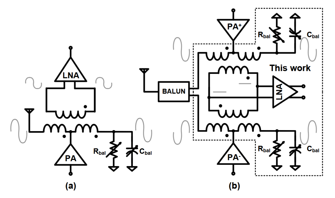
The terms "baluns", "transformers" and "hybrid transformers" are all refering to mutual inductances. Some academicians strictly associate these words with their contexts, but most people use these words interchangably today. In the duplexer shown in figure 4(a), the TX's PA is firing directly into a centre-tap of the bottom (B) side. Now this signal will be in common-mode across the ends of side B, so there is no differential across the ends now. Thus, the voltage developed across the top side will also be (ideally) negligible.
In 2018, Dr. Abhishek Kumar (now a Professor at IITH) and Prof. Aniruddhan (IITM) [3] proposed that instead of relying on tapping at different points to do the job, we use lumped capacitors for the bridge, as we will see in section 2.2. They showed that this also greatly improves the performance of the duplexer as we will see in section 2.4.
2.2. The Elephant in the Room
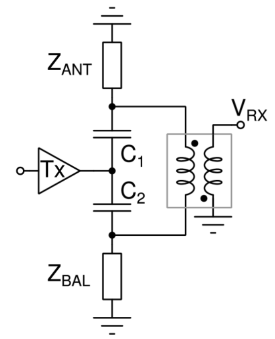
Let's address it rightaway: Figure 5 shows the duplexer used by Kumar et al. The current design at IIT Madras follows a very similar duplexer too. Follow [3] to find more about the multiple advantages they demonstrated with doing so.
2.3. Theory of Operation
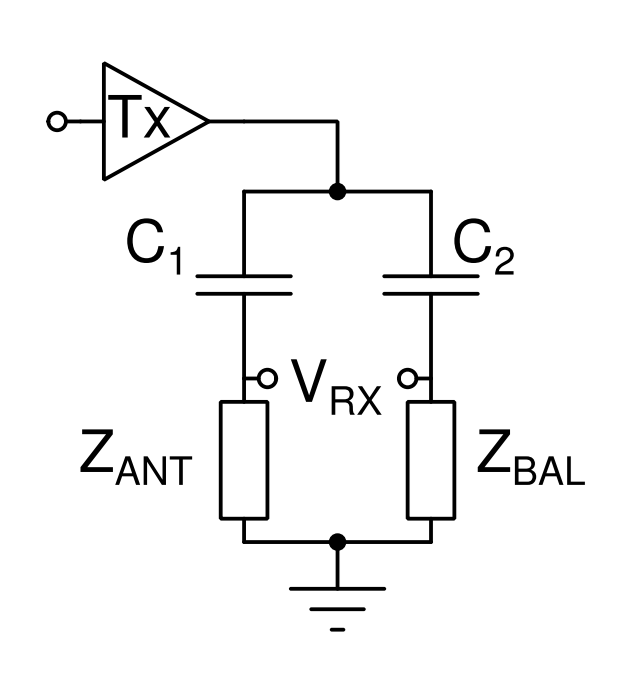
Why this works may not be trivial, so let's consider one perspective at a time, starting with the TX as shown in figure 6. Let's remove the balun for now. The signal developed between the C1 and Z_ANT will be equal to the signal between C2 and Z_BAL as long as C1·Z_ANT = C2·Z_BAL. (Note here that Z_BAL stands for "Balance Impedance", not to be confused with the "balun" transformer)
So if we read the RX signal differentially, the TX signal would become a common-mode, which can be cancelled if our RX chain has a high CMRR. Hence, we add the balun as shown in figure 5 to cancel the high TX swing before it reaches the LNA in the RX chain. In summary:
- TX Signal is seen as a common-mode across RX
- ANT Signal is seen in differential-mode across the RX after incurring a small loss, we'll call this "NF_RX"
- TX Signal reaches the Antenna after incurring a small loss, we'll call this "IL_TX".
This approach of making the bridge with capacitors and then having a balun fully decoupled from the bridge alleviates multiple design constraints that were imposed on the transformer earlier.
2.4. Is This Actually Better? - Performance Metrics
2.4.1. Is Cbridge better than Hybrid Transformer?
Shannon limit for continuous channels with gaussian noise dictates that the bitrate is upperbounded by B·log(1 + SNR). And SNR in the TX and RX paths will go down by factors of IL_TX and NF_RX respectively due to the losses. If we approximate (1 + SNR) ~ (SNR), then the total reduction in speed will have a factor of (IL_TX + NF_RX). Thus this quantity is taken as the performance metric for duplexers. [3] showed that using a C-bridge achieves better IL_TX + NF_RX than the hybrid transformers.
2.4.2. Is SCFD actually better than using two antennas normally?
For a fair comparison we should take two antennas in both cases and see which one achieves better bitrate. If we had two SCFD antennas, we would transmit and receive on both. So there is an additional factor of 2 on both RX and TX paths when we compare with 2x conventional FD antennas. And we have the losses dicussed above. So if we have IL_TX + NF_RX < 12 dB, then the design can be considered worthwhile.
(IL_TX + NF_RX) is taken to be the figure of merit for electrical balance duplexers
3. Why Should Z_BAL Be Tunable?
In any analog design, we need provisions to counteract PVT variations. Making Z_BAL tunable helps in this regard. But even if our fab promises us a nice TT-corner chip, there are other more compelling reasons to make it tunable:
3.1. Tracking Real Antenna
Z_BAL is actually the most critical block in SCFD, because the cancellation condition breaks down if the equality C1·Z_ANT = C2·Z_BAL breaks down. In introductory RF course, we assume that antennas are just 50 Ohm ports. But in reality, antenna can have wild impedance profiles.
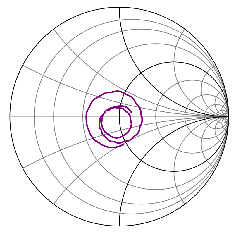
Above is an example of how an Antenna might look in a smith chart. If we plot the real and imaginary parts of the impedance against frequency, this will look like there are multiple peaks and troughs ranging anywhere from 30 to 80 Ohms. What's worse is that the antenna's profile can change with the environment around it. In fact, my personal experience is that just placing a table fan in front of an antenna being measured changes it's profile drastically!
Z_BAL is the most critical block in an SCFD IC and it has to track the antenna according to C1·Z_ANT = C2·Z_BAL across PVT variations and environmental conditions. Thus, Z_BAL has to be tunable
3.2. Oh, Just Adding Switches... Right?
Not quite, unfortunately! If the TX is blasting a power of +20 dBm (like most commercial ones do), the voltage swing across Z_BAL can exceed as much as 8V (if not 10V). Any MOSFET in modern technology nodes will get absolutely fried if we push 8 volts across Vds.
3.2.1. High-Voltage Highly-Linear Switches
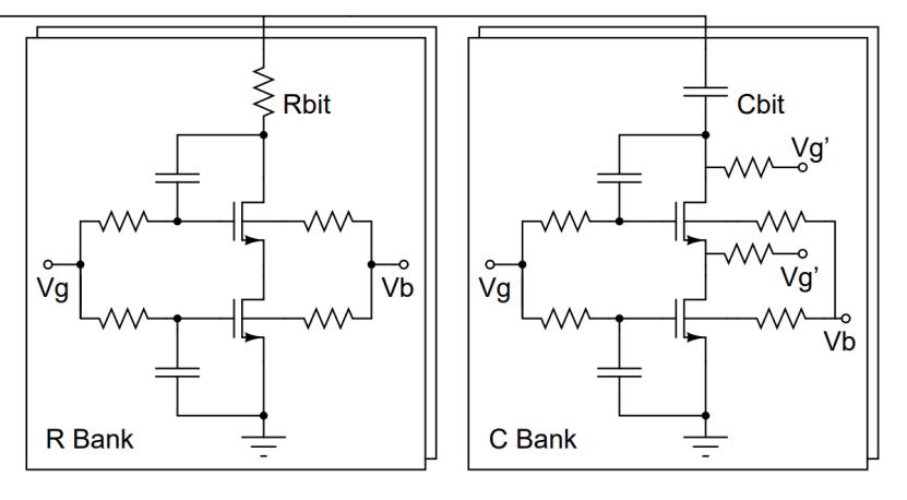
Kumar et al. [3] used a concept from [9] where FETs are stacked to withstand higher voltage by distributing the Vds seen. Further, G-S and G-D of the outer-most FETs are coupled at high frequency with additional capacitors for improved linearity. To read more upon this simple but brilliant concept in detail, follow [9]. In short, coupling G-S makes sure the ON/OFF state of the bottom FET is reliably maintained. Coupling G-D makes sure that the top FET does not enter saturation or cut-off unexpectedly.
3.2.2. So... Just Stacking FETs?
In the process node that [3] used, stacking two thick oxide FETs sufficed because each FET could withstand 3.3V. But in the process node currently being used, the same swing would need 4 FETs, and this would severely damage the quality of the switches. This calls for a different solution! But I won't disclose much here ;)
The switches used in Z_BAL must endure the high TX swing seen. They also have to be highly-linear to avoid feedthrough of higher harmonics of TX signal into RX.
4. What's Currently Brewing in Research?
So far we discussed SCFD like a glorious solution which can instantly give us atleast 1.5x the bitrate for the same number of antennas. Then why isn't this in production yet? Is there something we forgot? Here are some hints (although the next heading might give it away):
- We didn't yet discuss about what happens with the "B" term in the Shannon limit
- Some modern OFDMA bands can be as wide as 160 MHz [2]
4.1. Wideband Operation
Bandwidth of operation is a major concern in SCFD systems. The primary bottleneck is the range of frequencies for which Z_BAL reliably tracks Z_ANT. [3] achieved a 10 MHz (single-sided) bandwidth at 2.5 GHz. The closest to a wideband operation was shown by [5] with their "dual notch" solution, which achieved 80 MHz at 1.9 GHz, but they had to pay their price in the NF_RX.
Bandwidth to which Z_BAL tracks Z_ANT is the bottleneck for wideband operation of electrical balance duplexers
D. Regev et al. [10] showed mathematically that a multi-resonant Z_BAL would be necessary for wideband cancellation. Fortunately, we believe that solving the problem discussed in section 3.2.2. would also enable multi-resonant Z_BAL implementations as an added advantage!
The design of a multi-resonant Z_BAL that achieves high tunability under high-voltage stress remains an avenue for further development
5. The Future?
Translating ideas into silicon remains fundamental to RF IC research. The ideas discussed in this article form the basis of ongoing work at IIT Madras. As part of this effort, my work with Prof. Aniruddhan has translated some of these ideas to the pre-silicon stage, while others remain open for exploration. Future work will focus on pursuing the remaining ideas, and the fabrication and silicon validation of these concepts. We hope this article provides a good overview of the current full-duplex landscape! If this area interests you, feel free to reach out to us!
References
[1] Dahlman et al., IEEE Comm Mag, Apr 2009
[2] Prof. David Koilpillai, EE6143: Advanced Topics in 5G Communications, IIT Madras, Aug 2024
[3] A. Kumar and S. Aniruddhan, "A 2.5-GHz CMOS Full-Duplex Front-End for Asymmetric Data Networks," in IEEE Transactions on Circuits and Systems I: Regular Papers, vol. 65, no. 10, pp. 3174-3185, Oct. 2018, doi: 10.1109/TCSI.2018.2809924
[4] B. van Liempd, J. Craninckx, R. Singh, P. Reynaert, S. Malotaux and J. R. Long, "A Dual-Notch +27dBm Tx-Power Electrical-Balance Duplexer," ESSCIRC 2014 - 40th European Solid State Circuits Conference (ESSCIRC), Venice Lido, Italy, 2014, pp. 463-466, doi: 10.1109/ESSCIRC.2014.6942122
[5] S. H. Abdelhalem, P. S. Gudem and L. E. Larson, "Tunable CMOS Integrated Duplexer With Antenna Impedance Tracking and High Isolation in the Transmit and Receive Bands," in IEEE Transactions on Microwave Theory and Techniques, vol. 62, no. 9, pp. 2092-2104, Sept. 2014, doi: 10.1109/TMTT.2014.2338271
[6] B. van Liempd, P. Wambacq and J. Craninckx, "An inductorless electrical-balance 360° phase shifter for 0.5-1.15GHz in 0.18μm CMOS," 2015 10th European Microwave Integrated Circuits Conference (EuMIC), Paris, France, 2015, pp. 132-135, doi: 10.1109/EuMIC.2015.7345086.
[7] E. F. Sartori, "Hybrid Transformers", IEEE Transactions on Parts, Materials and Packaging, Vol. pmp-4, No. 3, Sep 1968.
[8] M. Mikhemar, H. Darabi and A. Abidi, "A tunable integrated duplexer with 50dB isolation in 40nm CMOS," 2009 IEEE International Solid-State Circuits Conference - Digest of Technical Papers, San Francisco, CA, USA, 2009, pp. 386-387,387a, doi: 10.1109/ISSCC.2009.4977470.
[9] M. Ahn, H.-W. Kim, C.-H. Lee, and J. Laskar, “A 1.8-GHz 33-dBm P 0.1-dB CMOS T/R switch using stacked FETs with feed-forward capacitors in a floated well structure,” IEEE Trans. Microw. Theory Techn., vol. 57, no. 11, pp. 2661–2670, Nov. 2009.
[10] D. Regev, R. Keren, N. Ginzberg and E. Cohen, ”Fano-Bode Cancellation-Bandwidth Limit in Full-Duplex Wireless Transceivers,” in IEEE Transactions on Circuits and Systems I: Regular Papers, vol. 71, no. 12, pp. 6507-6520, Dec. 2024, doi: 10.1109/TCSI.2024.3420419